![]()

UTBI: Under The Background Influence
Development
![]()
![]()
![]()
![]()
![]()
The Electronics
In a semiconductor material, the incident radiation can create a very large number of electron-hole pairs since the energy required to produce one electron-hole pair is small (about 3 to 6 eV), depending on the band gap and the properties of the material being employed.
For our experiment, we will be using a CdZnTe semiconductor material which has very small leakage current at room temperature (pA) due to the addition of Zinc to a standard CdTe material.
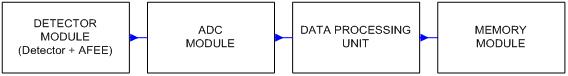
The events detected by the CdZnTe detector will be amplified, sampled and band discriminated in the Analogue Front End Electronics (AFEE). The signals coming from the Detector Module are digitalized in the ADC (Analogue to Digital Converter) modules. The digital signal is time and channel tagged by the FPGA. Finally, the data is stored in the secondary memory.
Main devices:
Simplified block diagram:
1.- Detector Module:
The detector is based on a CdZnTe with dimensions 1.5x1.5x0.75 cm3. The AFEE will be implemented in an ASIC device. The detector and the AFEE will perform the Detector Module (DM). The DM will be supplied by eV Products. The DM is a new development from the current Coplanar Grid Detector (CPG). The main characteristics of the CPG detector module are:
• Input Voltage: 2.5 V
• Bias Voltage: 1000 V
• Energy range: 30 keV-10 MeV
• Peaking time and gain adjustable
2.- Analogue to Digital converter (ADC)
The ADC links the detector module (analog) with the data processing unit. It can be considered as the DFEE (Digital Front End Electronic) as it is shown in the block diagram. The most important features are shown below:
• Model AD7914
• 10 bits
• Fast throughput rate: 1 MSPS
• Conversion time: 800ns (max)
• 4 channel
• Serial output(Features may change as a result of the design process.)
3.- Universal Time Clock (UTC)
UTC block allows the association of a time tag with every sample coming from DFFE. The resolution must be at least as the ADC´s sample time.
4.- Process Unit
All the operations are managed by the FPGA (Field Programmable Gate Array). As it is a concurrent based device, it allows different processes running at the same time. The “datapath” and the “controlpath” will be embedded in the same device in order to avoid hardware complexity, integrity signal problems etc…
5. Storage
Acquired data will be saved in a storage memory (secondary memory). MicroDrives are designed for working in vibration environments like mobile devices (cameras, camcorders etc). The storage device needs a controller which acts as interface with the Process Unit. The controller type can be hardware or software. The interfacing with secondary memory represents the most delicate part of the design.